if “STM32F40_41xxx” in extra_flags:
src_filter_patterns += [“-“]
if “STM32F427_437xx” in extra_flags:
src_filter_patterns += [“-“]
elif “STM32F303xC” in extra_flags:
src_filter_patterns += [“-“]
elif “STM32L1XX_MD” in extra_flags:
src_filter_patterns += [“-“]
elif “STM32F10X_MD” in extra_flags:
src_filter_patterns += [“”]
5. Make a folder named stm32f1 under /Users/yinhuanyuan/.platformio/packages/framework-spl/stm32/cmsis/variants
startup_stm32f10x.c
stm32f10x.h
stm32f10x_conf.h
system_stm32f10x.c
system_stm32f10x.h
6. Make a folder named stm32f1 under
/Users/yinhuanyuan/.platformio/packages/framework-spl/stm32/spl/variants
make a folder named inc and src under this stm32f1 folder.
7. Copy the following files to inc folder
misc.h
stm32f10x_adc.h
stm32f10x_bkp.h
stm32f10x_can.h
stm32f10x_cec.h
stm32f10x_crc.h
stm32f10x_dac.h
stm32f10x_dbgmcu.h
stm32f10x_dma.h
stm32f10x_exti.h
stm32f10x_flash.h
stm32f10x_fsmc.h
stm32f10x_gpio.h
stm32f10x_i2c.h
stm32f10x_iwdg.h
stm32f10x_pwr.h
stm32f10x_rcc.h
stm32f10x_rtc.h
stm32f10x_sdio.h
stm32f10x_spi.h
stm32f10x_tim.h
stm32f10x_usart.h
stm32f10x_wwdg.h
copoye the followign files to src folder
misc.c
stm32f10x_adc.c
stm32f10x_bkp.c
stm32f10x_can.c
stm32f10x_cec.c
stm32f10x_crc.c
stm32f10x_dac.c
stm32f10x_dbgmcu.c
stm32f10x_dma.c
stm32f10x_exti.c
stm32f10x_flash.c
stm32f10x_fsmc.c
stm32f10x_gpio.c
stm32f10x_i2c.c
stm32f10x_iwdg.c
stm32f10x_pwr.c
stm32f10x_rcc.c
stm32f10x_rtc.c
stm32f10x_sdio.c
stm32f10x_spi.c
stm32f10x_tim.c
stm32f10x_usart.c
stm32f10x_wwdg.c
然而,以上只是高地族群历史的一个面相,并不能代表高地族群国家化进程的全部。笔者认为,斯科特在认识高地族群与国家的关系方面,过于强调两者的对立,而低估了二者之间合作的可能性。例如,斯科特认为,在差不多两千年的时间里,中原王朝扩张的压力造就了一个将人口不断推向山地的单一历史过程。尽管这一压力时有时无,但总是朝着一个方向(James C. Scott,2009:142)。由此可见,在斯科特看来,国家总是单一地迫使低地人群向高地迁徙,而难以见到相反的运动轨迹——即高地族群选择融入国家所控制的低地。在谈到高地族群内部竞争时,斯科特亦强调后来进入高地的族群若军事实力较强,则会迫使原来的族群向更高的地方迁徙;若后来者实力有限,往往只能占据那些位于高处的小块地带(James C. Scott,2009:140—141)。
It is little secret I use a ton of Python to get tasks in ArcGIS done. If serious about getting volumes of data processed with ArcGIS, Python is far and above the way to get things done quickly. If you start venturing far into this world, you will discover a whole raft of great modules created by a healthy community of Python developers available through what is referred to as the Python Package Manager or as it typically known by the command line command, pip.
The idea is simple enough. Python maintains a library of modules anybody can automatically download and use. All you have to do is open up a command line prompt and type pip install <package-name>. It all sounds so easy. The is one little problem. Python packages can be built with and frequently do include C++ code. This C++ code needs to be compiled. Linux and Mac have this decently covered. Windows however, is a gigantic pain to get this working on. This is the Windows challenge. It does not end here, though.
When ArcGIS for Desktop (ArcMap and ArcCatalog) are installed, Python 2.7 32-bit is installed in C:\Python27\ArcGIS10.3. When Background Geoprocessing is installed, Python 2.7 64-bit is installed in C:\Python27\ArcGISx6410.3. If you are like me and also install ArcGIS Pro, you also get Python 3.4 64-bit installed in C:\Python34. Hence, if you have all of ArcGIS for Desktop installed, you have three versions of Python installed and three places where you can theoretically access pip.
Thus, our challenge is two-fold. First, we need a way to compile C++ so we can install Python packages. Second, even if we can compile and install packages, we need to figure out a way to access pip for each Python installation.
Addressing compiling, you can download and install the Windows SDK from Microsoft. This will provide the compiler and other resources needed to compile the packages. When installing, the thing you really need is the C++ compiler. Why this is not better documented someplace, I have no clue. It is a gigantic pain to figure out.
Next up is the challenge of finding and using pip for each of our three installations. Two have it already installed. One does not.
The two installations with pip and the respective locations are:
To install packages found in the Python Package Repository, we can now find something useful such as ArcREST, navigate to each of the installations’ Scripts directory and install the package. Hence, for ArcREST:
> cd C:\Python27\ArcGIS10.3\Scripts
> ./pip.exe install arcrest
> cd C:\Python27\ArcGISx6410.3\Scripts
> ./pip.exe install arcrest
> cd C:\Python34\Scripts
> ./pip.exe install arcrest
Redundant? Yes, a little. But now at least you can get packages installed consistently across all three Python installations on your machine!
Can’t afford a Chromebook? Looking for an alternative to Raspbian? Here’s how to install a version of Chrome OS on your Raspberry Pi.
Fancy a look at Chrome OS without spending money on a new computer? Wondering if a cloud operating system might improve the Raspberry Pi’s performance as a productivity tool? Wonder no more—it’s possible to install Chrome OS on the $50 computer and find out how well it runs.
You’re presumably running the latest version of Raspbian on your Raspberry Pi. But is it the best Linux distro for the device? Could there be an alternative that you might find suits you better?
But Chrome OS offers something different: cloud computing. The relatively low specification of the Raspberry Pi makes it ideal for Chrome OS. The operating system is designed to run most of its software as web apps, relying on servers for the processing.
Another reason to install Chrome OS on the Raspberry Pi is that it is easy to use. Google has spent years polishing and perfecting the operating system. These changes have been felt in the official release as well as the open source Chromium OS.
The Open Source Chrome OS
While Google manages and releases Chrome OS, the operating system is based on an open source project, Chromium OS. This has been released on various devices, and thanks to the FydeOS project can be installed on the Pi.
Note that several other versions of Chromium OS have been released on the Raspberry Pi. These are now discontinued; there is every chance that FydeOS might be abandoned in future. As such, you may prefer to download and build from the original source code available at www.chromium.org.
For this tutorial, we’re going to use the preconfigured code available in FydeOS.
Grab These To Install Chrome OS On Raspberry Pi
To install and run Chrome OS on a Raspberry Pi computer, you’ll need:
A Raspberry Pi 3 or 3B+ (there is no working image for the Pi Zero, or for the Raspberry Pi 4)
Along with a mouse, keyboard, HDMI cable, and spare display, you’ll be ready to get started with Chrome OS.
Prepare Your SD Card For Chrome OS
The downloaded IMG file is compressed in XZ format, so you’ll need to expand this with a suitable tool. 7-Zip is your best option on Windows; XZ can be expanded natively on Linux systems.
Next, the IMG file needs to be written to the SD card. The simplest option here is the excellent Etcher tool, which will also format your SD card. Download, install, and run Etcher, then click Select image to browse for the Chromium IMG file.
Following this, confirm that the microSD card is detected by Etcher. If not, reinsert the media in your PCs SD card reader and wait until it shows up.
Finally, click Flash to write the data. A few minutes later, Chrome OS will be installed on the microSD card, ready to boot.
Booting Chrome OS On The Raspberry Pi
After safely removing the microSD card from your PC it will be ready to boot in your Raspberry Pi.
The first boot may take a while to complete. You’ll then be prompted to complete the set-up steps. If you’ve used a Chromebook or Android device, you’ll recognize this. It’s basically a case of inputting (or creating) your Google account details.
Once logged in, you’ll see a bare desktop, ready to be configured. You’ll find the launcher in the bottom-left corner and the notifications in the bottom-right. Everything should feel in some way familiar.
You will notice that Chrome OS on the Raspberry Pi does not quite resemble the version seen on a Chromebook. For example, the Launcher icon on the Shelf is a circle, rather than a 3×3 grid. This is largely cosmetic, however, and makes no difference to the functionality of the OS.
Wondering what your first step should be? Right-click the desktop and select Set wallpaper.
With a stunning background set, you’ll be ready for anything!
Will Chrome OS Software Run On The Raspberry Pi?
Various apps will come pre-installed with the Raspberry Pi version of Chrome OS, as they would with the main release. For example, when I signed in with my usual Google account, I had the Photos app, Google Keep, and more.
This shouldn’t come as much of a surprise. The Chrome OS is based on Linux and supports primarily web applications. “Web apps” are platform-agnostic, relying on a web browser to run.
Almost all Chrome OS apps will run on the Raspberry Pi—none have been found so far that don’t. Looking for suggestions beyond the usual Chrome OS options? Try our list of essential apps for your new Chromebook.
Does It Feel Like A $50 Chromebook?
Chromebooks are affordable computers, typically in the $150-$1500 price range. Installing Chromium OS on the Raspberry Pi with FydeOS gives you the opportunity to build your own Chromebook.
What’s more, you’re likely to only need to spend $50 for a new Raspberry Pi. While it won’t be as fast as the top end Chromebooks, Chromium OS on the Raspberry Pi is certainly on par with the cheaper Chromebook devices.
Once you’ve installed all your preferred productivity apps for Chrome OS, you’ll be ready to go. Need help? Try our Chrome OS cheat sheet for tips.
A Budget Productivity Pi With Chrome OS
The Chromebook range of computers and Chrome OS have been the biggest challenge to Microsoft and Apple over the past decade. Could they really replace standard desktop and laptop computers?
It remains difficult to tell. But you can certainly find out if Chrome OS is something you’re interested in. Simply follow the steps above to install the parent operating system, Chromium OS, on your Raspberry Pi with FydeOS. You can even install ChromeOS on a virtual machine.
Top 18 Flutter Maps Widgets Package you Should Know
1.Search Map Place
This is a Flutter package that uses the Google Maps API to make a TextField that tries to autocomplete places as the user types, with simple smooth animations, providing a nice UI and UX. This will also provide great information about the user selected place, like the coordinates, the bounds to determine the zoom of the GoogleMap widget, and so on.
A Flutter package that provides a native map to both Android and iOS devices.
The plugin relies on Flutter’s mechanism for embedding Android and iOS views. As that mechanism is currently in a developers preview, this plugin should also be considered a developers preview.
This package combines the google_maps_flutter plugin with apple_maps_flutter to create a cross platform implementation of native maps for Android/iOS.
A Flutter plugin which provides ‘Picking Place’ using Google Maps widget.
The project relies on below packages.
Map using Flutter’s official google_maps_flutter Fetching current location using Baseflow’s geolocator Place and Geocoding API using hadrienlejard’s google_maps_webservice Builder using kevmoo’s tuple
A Flutter plugin that provides an Apple Maps widget.
The plugin relies on Flutter’s mechanism for embedding Android and iOS views. As that mechanism is currently in a developers preview, this plugin should also be considered a developers preview.
This plugin was based on the google_maps_flutter plugin. Instead of reinventing the wheel it also uses the Flutter implementation of the google_maps_flutter plugin. This was also done to simplify the process of combining the google_maps_flutter plugin with apple_maps_flutter to create a cross platform implementation for Android/iOS called flutter_platform_maps.
A map widget with live position updates. Based on Flutter map and Geolocator. Provides a controller api to handle map state changes.
Note: the map controller api has been moved to the map_controller package. The Livemap controller package is now only responsible for the geolocation related controls
Localizator is a flutter application that provides your current/given position,and gives you weather Forecasts Locativity is a flutter application implements flutter_map and Geolocator plugins to provide your current/given position then render it on a map. View on GitHub
15.Maps Demo
A Flutter example to use Google Maps in iOS and Android apps via the embedded Google Maps plugin Google Maps Plugin. View on GitHub
Please note that this project is experimental and is not officially supported. We welcome feedback and contributions.
This Flutter plugin for mapbox-gl-native enables embedded interactive and customizable vector maps inside of a Flutter widget. This project plugin is in early development stage. Only Android is supported for now.
Toolchain for the Longan Nano on the Raspberry Pi 3
Thanks to Kevin on www.susa.net for pointing me in the right direction. Because i couldn’t get the riscv-nuclei-elf-gcc i had to do the following on a x86 debian machine. Here are all the steps i have done:
At Charlie foxtrot we aim to stay relevant and keep up with new and exciting tech. So how do we do that? We experiment! This time we wanted to capitalize on our in-house competence in Flutter and Rust. Our Flutter expert, Jonathan, had read about Darts foreign function interface (ffi) capabilities and wanted to try it in conjunction with Rust. He asked me if I thought if we could build something that would run on a Raspberry pi (rpi). Without having a clue, I said “YES!” and got to work. The resulting code can be found here.
After some debating, we landed in an idea where we would have a Flutter interface that let the user take a photo via the rpi camera module and then display the image in the app. This is a simple app but considering that Flutter don’t have official support for the rpi, this could be quite the challenge. We also decided to build a small (read: very small) library in Rust to communicate with the camera.
First thing to do is to set up the Raspberry Pi. In the README of the flutter-pi repo it’s mentioned that flutter-pi should run without Xserver. Therefore I went with a headless version of RaspberryOS. Once you’ve flashed the os to a ssd card, follow the instructions in the flutter-pi README and install drivers for your touch screen of choice. Be sure to clone the engine-binaries branch of flutter-pi and place the files in the correct directories aswell.
On the software side we first want to set up Flutter on our laptop. If you are using a linux distro you may have the option to install and run Flutter via snap. I found that this leads to several issues. Because of that I cloned the Flutter repo from Github and installed it manually. Where you install Flutter doesn’t really matter as long as you put /flutter/bin in your $PATH.
Next you want to make sure you are using a Flutter version that’s compatible with flutter-pi. At the time of writing this the compatible version is 1.22.2. You can change Flutter-version by checking out the corresponding branch. You can now test your installation by running flutter create <name> followed by flutter build bundle. If it builds without errors, everything should be correct.
We will also need to install Rust so that we can build the small library that lets us talk to the camera. Do this by going over to the Rust website and follow the instructions. Once Rust is installed we need to add the armv7 target for the rust compiler in order for us to cross compile the code. Do this with: rustup component add rust-std-armv7-unknown-linux-gnueabihf. Now create a Rust project using cargo new –-lib ffi-test. The last part (ffi-test) is the name of the project and doesn’t matter, choose a name to your liking. As I mentioned earlier we need to cross compile the code since it’s going to run on the rpi and not the machine we are writing the code on. Create a directory called .cargo and place a file in there named config.toml. In that file place the following:
The last part after “linker =” is the gcc linker for arm. Install this if you don’t already have it on your machine. Google the correct name of the package for your distro. The name displayed here is the package name on Manjaro. We also need to declare, inside the Cargo.toml, that we want to build a dynamically linked library (.so) like this:
[lib]
name = "ffi_test"
crate-type = ["cdylib"] #dynamic library
The next logical step would be to build a small “Hello world” library in Rust and consume it from Dart/Flutter. Lets create a function that returns a hard coded string when called.
#[no_mangle]
pub extern fn string_from_rust() -> *const c_char {
    let s = CString::new("Hello from Rust!").unwrap(); // Create a CString from "Hello world"
    let p = s.as_ptr(); // Get a pointer to the underlaying memory for s
    std::mem::forget(s); // Give up the responsibility of cleaning up/freeing s
    p
}
Since Dart’s ffi mechanisms utilizes the C ABI, we need to annotate the Rust function with #[no_mangle] in order to preserve the function signatures symbol upon compilation. Since we are compiling this into a .so we need to mark the function as extern so that it can be linked as any other library. The functions return type is *const c_char, which is a raw pointer, basically a raw memory adress. We have to do this since Rust’s types are not available in Dart. When we send data over to Dart, Rust can no longer take responsibility for cleaning up that data. Rust no longer have the required information regarding that data’s usage and could therefore free the data at an inappropriate time. To build this just run cargo b
Now we want to consume the Rust function from the Dart side of the project. To do that we need the following dependencies:
We first load the .so library we compiled from Rust, we look up the function and store it in the state. We then write a small helper function that will call the _string_from_rust_ffi-function. Then we have to encode the string returned from Rust to UTF8 using Utf8.fromUtf8().
In order to test this enable desktop support with:
Check the config with flutter devices and see that your os shows up. Then to run the app run flutter run -d linux. You should something like this:
Moving over to the Rpi
The main goal in this post is to get Flutter running on the rpi while consuming a Rust library. So far we haven’t run anything on the rpi. Lets fix that!
Flutter does not have any official support for rpi, that’s why we need to use the aforementioned flutter-pi. If you have followed the instructions in the repo for flutter-pi you should have it installed on the rpi. It would be ideal if we could just take the code we built earlier and throw it on to the rpi and run it. Unfortunately that’s not the case. The engine-binariesbranch from the flutter-pi repo needs to be cloned to the “host” (the computer you are coding on) in order for us to build and compile the Flutter app. Once you’ve done that go through the build steps in the README of flutter-pi. To save myself time I’ve saved these as bash scripts. These are listed below.
To run the application ssh into the rpi and run flutter-pi flutter_hello_world_assets. If all goes well you should see the “Hello world” app from Flutter and once you press the button the text changes to “Hello from rust.
Incorporating the camera
Now that we know how to compile and run Rust and Flutter in conjunction on the rpi we want to be able to control the camera from our app. There might be libraries for controlling the camera written in Dart but since we want to use Rust together with Dart, we’re going to do it from Rust.
I’ve chosen a library called rascam. It’s a small library built on top of mmal-sys. We can add rascam to our Rust project by adding this to the Cargo.toml file:
[dependencies]
rascam = "*"
Now lets take a look at the code for taking an image.
// ffi-test/src/lib.rs
use std::ffi::CString;
use std::os::raw::c_char;
use rascam::*;

// ...

#[repr(C)]
pub struct ImageBuffer {
    img_ptr: *mut u8,
    len: u32,
}

#[no_mangle]
pub extern fn take_photo() -> *mut ImageBuffer {
    let info = info().unwrap();
    if info.cameras.len() < 1 {
        println!("Found 0 cameras. Exiting");
        // note that this does not run destructors
        ::std::process::exit(1);
    }
    println!("{}", info);
    let mut camera = SimpleCamera::new(info.cameras[0].clone()).unwrap();
    camera.activate().unwrap();
    let mut bytes = camera.take_one().unwrap();
    let len = bytes.len() as u32;
    let ret = bytes.as_mut_ptr();
    std::mem::forget(bytes);
    let mut ib = Box::new(ImageBuffer { img_ptr: ret, len});
    let ret = Box::into_raw(ib);
    std::mem::forget(ret);
    ret
}
There is a lot going on here. If youve never ventures in to the unforgiving territory of low level Rust, this might look a little daunting. But fear not! I will explain it all, piece by piece.
On a high level this code solves two problems, take a photo and send it to whoever is calling the function. We will start with the second problem, sending the photo to the caller. Since it’s just two values we we want to pass on, one might be tempted to utilize a tuple like (*mut u8, u32). This is however not a viable option since the memory layout of a tuple in Rust is not guaranteed. So we went with a simple struct. The #[repr(C)] tells the compiler to treat the struct as a C struct. This means that the fields of the struct will be aligned the same way in memory as we declared them in the code. We need this because the C ABI being the common grounds for communication between Rust and Dart.
We start with getting the necessary info for the camera. We use this to check if there even is a camera to begin with. If there isn’t we just close the process.
  let info = info().unwrap();
  if info.cameras.len() < 1 {
      println!("Found 0 cameras. Exiting");
      // note that this does not run destructors
      ::std::process::exit(1);
  }
  println!("{}", info);
We then instatiate the camera using the info and activate it.
 let mut camera = SimpleCamera::new(info.cameras[0].clone()).unwrap();
 camera.activate().unwrap();
We take a photo, get the number of bytes, get a pointer to the byte array and tell the compiler to forget about the byte array. Just as with the string earlier this array will be cleaned up by Dart.
  let mut bytes = camera.take_one().unwrap();
  let len = bytes.len() as u32;
  let ret = bytes.as_mut_ptr();
  std::mem::forget(bytes);
Next we create an ImageBuffer and place it on the heap by wrapping it in a Box. If we didn’t place it on the heap and still returned a pointer to it, the ImageBuffer would be popped of the stack once the function call returns. That would make it possible for the memory to get overwritten while Dart uses the pointer. We don’t want that!
  let mut ib = Box::new(ImageBuffer { img_ptr: ret, len});
  let ret = Box::into_raw(ib);
  std::mem::forget(ret);
  ret
With that everything is well and done on the Rust side but how do we actually use this in Dart? First will need to declare a type to represent the ImageBuffer in Dart.
class ImageBuffer extends Struct {
  Pointer<Uint8> img_ptr;

  @Uint32()
  int len;
}
then we need a type for the actual function providing us the ImageBuffer and we need to look it up in the library:
We then declare a function to be called on button press:
  void _takePhoto() {
    setState(() {
      _imageBuffer = _take_photo_ffi().ref; // _imageBuffer is a member of our state
      _counter++;
      _message = "Photos taken: '$_counter'";
    });
  }
Once all that is done we can register the function with the button:
  // Inside a widget array in a scaffold
  if (_imageBuffer != null)
    Image.memory(_imageBuffer.img_ptr.asTypedList(_imageBuffer.len)),
Unfortunately I couldn’t build the Rust library on my Linux machine because of mmal-sys. There might be a solution for this. But to build this I:
pushed the Rust library code to github
built the flutter bundle on the host, using the scripts
uploaded it to the rpi and ran it. It then gave me this:
Now you should hopefully have a Flutter app running on a rpi!
Takeaways
For me the main takeaway is that our approach here might actually be a viable option for resource scarce devices. The possibility of writing a beautiful, interactive application in Flutter and have run in a car infotainment system for example is quite exciting. The possibility to handle the low level stuff with languages such as Rust and C, really opens up this domain for Flutter. I at least know that I am waiting for official rpi support for Flutter so that I can build something more robust!
All the other projects I have made so far have been digital and microcontroller based, with the one exception to this being the Nutclough amplifier, which was assembled from a kit. The big difference in this project is that unlike the other ones which I have built from scratch it is an analogue RF circuit.
We already had some TA7642 AM receiver ICs in the workshop and some PP3 battery clips to hand, so I wanted to use both of these components in my circuit. Since I had never built any analogue circuits before I wanted to keep this fairly simple so would use an external test audio amplifier for testing.
After doing a bit of research it became apparent that a very important part of the radio is a tuned circuit, which can be tuned to a particular frequency in order to select the radio station desired. This can be made from an inductor and a variable capacitor connected in series or parallel.
I began looking for examples of circuits for the TA7642 and the majority used either a 1.5v or 3v supply. I occasionally found ones which used a 9v battery, however most of these seemed to incorporate built in amplifiers. After a bit more searching I finally found one which did not.
This circuit consists of:
– 1 x 9v battery – 1 x 10k resistor – 1 x 1k resistor – 1 x 100k resistor – 2 x 1n4148 diode – 1 x .01uf capacitor – 1 x .1uf capacitor – 1 x 470uf+ capacitor – 1 x 1uf+ capacitor – 1 x TA7642 IC – 1 x ferrite coil antenna – 1 x variable capacitor – 1 x test amplifier – 1 x switch
I decided not to include a switch, as I could just remove the battery, so I removed the switch from the schematic. The ferrite coil antenna which I had had both a long wave and a medium wave coil on separate formers on the ferrite rod, each coil consisted of a longer coil and a shorter coil too. So there were four coils in total.
I began connecting the components as above in the schematic, using a breadboard. When I powered up the circuit I could hear a muffled radio station, but when I adjusted the capacitor nothing changed and it should have done.
I checked the layout against the schematic again and then powered up the circuit to find the same result. I then checked the values of all the resistors and capacitors for errors, here I found I had accidentally used a 100 ohm resistor instead of 100k. I replaced this and powered up the circuit once more hoping this would resolve the problem, but again it didn’t.
When I initially began looking at tuned circuits many of them only used a single coil of one length. So I then wound my own ferrite antenna using enamel wire and I attempted wiring my circuit with this.
The circuit didn’t work with this coil, so I tried again using the original medium wave coil, but this time not using the shorter winding. Instead by connecting the longer winding and variable capacitor in parallel and directly in circuit.
When the circuit was powered up this time it surprisingly worked! Varying the capacitance tuned the circuit and the radio was now quite clear to listen to.
I’m still unsure as to why the radio circuit didn’t work the first time and I will look into this further to try understand what went wrong.
Another fun project as I learn more about electronics!
In this post we comprehensively learn a step wise process of making small DIY PCBs at home through minimum effort and maximum precision.
DIY Step-wise Procedures
It basically involves the following crucial steps:
Cutting copper clad laminate into proper size.
Punching indentations for drilling holes for the component leads, as per the schematic.
Drawing pads around the indentations with etch resist paint, and linking the pads through tracks using etch resist paint.
Immersing the painted board in ferric chloride solution, until the chemical eats away the exposed copper, leaving the painted layout sections intact.
Drying the board and scrubbing out the etch resist paint from the tracks and the pads.
Drilling holes on the indentations.
Polishing the finished board with fine emery paper.
Using the ready PCB for assembly and soldering the parts.
Now let’s discuss the above steps in details. The first step in PCB production would be to acquire the essential resources and items. We are going to focus on all those things that are fundamental.
Materials Needed for Making PCB
To start the process we will first gather all the vital ingredients or materials required for the PCB making. The following fundamental things will be needed for the production
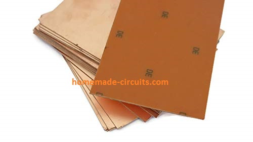
Copper Clad Laminate
Ferric Chloride Solution
Etch Resist Chemical or paint.
Painting brush or Pen
Container for etching the PCB
Drill Machine and Drill Bit.
Etchant Remover
Scouring pad, Kitchen Paper
Copper Clad Laminate
The most basic item will be the copper clad for making the printed circuit board alone, and you will find a variety of these.
The base (insulating) stuff is generally either fibreglass or SRBP (sheet resin bonded paper), and the latter is usually the more affordable option.
However, fibreglass has become the widely used both with commercial and recreational consumers as it is equipped with a couple of positive aspects.
The first is basically that it is tougher and for that reason less susceptible to bending and breaking than SRBP. The improved durability is additionally very helpful for boards that bear weighty parts for example transformers.
An additional benefit is that fibreglass is translucent and thus typically allows us to view the copper paths through the top (component) area of the board which is often worthwhile when examining and fault-finding.
Having said that, the standard of SRBP boards is more than satisfactory for many requirements. Marketing campaigns usually make reference to board as 1mm, 1.6mm, etc., and this is actually refering to the thickness of the base material.
Board Thickness
Naturally the thicker (about 1.6 to 2mm) boards tend to be more robust compared to slimmer (about 1mm) models, however the heavier quality boards are only crucial for large PCBs, or where weighty parts will likely be installed on the board.
For the majority of applications the thickness of the board is actually of little consequence.
Occasionally copper laminate board will likely be chosen as one ounce quality, or possibly two ounce quality, which appertains to the weight of the copper on one square foot of board.
Most circuits deal with just quite low currents, and regular one ounce board is just about all that’s needed. In reality one ounce board is frequently satisfactory even for circuits involving formidable currents.
The Etch Resist Paint
The etch resist is subsequently taken off to expose the copper tracks and pads.
Whichever paint that is able to keep the etchant away from the copper layout during the etching process can be employed as the resist.
I personally prefer using nail enamels or nail polish, any cheap brand can be used and will work great as an etch resist.
Properties of Etch Resist
Professionally, probably the most widely used resists are waterproof paints and inks. Water soluble varieties are definitely not fit for purpose simply because these an get dissolved and washed off in the etching solution.
A paint or ink that dries quickly is more advantageous because it eliminates the need to wait for a long time before the board could be etched.
Even the more basic printed circuit patterns appear to have a large quantity of thin copper tracks within a relatively compact area of board nowadays, and a paint brush competent at creating extremely fine lines becomes necessary.
Drawing the Track Layout
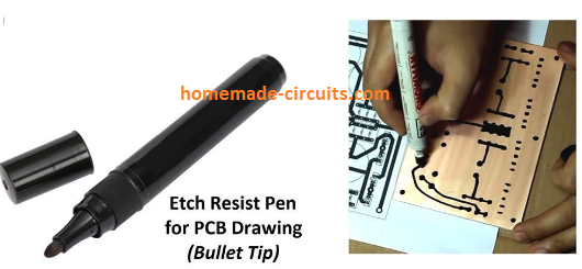
A simple solution would be to utilize an worn-out fibre-tip pen in paint brush manner, which can help develop outstanding final results although it might not look like quite a exquisite means to fix the issue. An easier way of implementing the resist is to use one of the commercially available etch resist pens which can be easily bought from any electronic part dealer.
Any kind of pen that uses a spirit based ink and a sharp point should be workable with this application. In case you are uncertain regarding the appropriateness of a pen you can easily pull out a few traces over a discarded copper laminate board then etch the board to verify if the ink maintains the etchant away correctly.
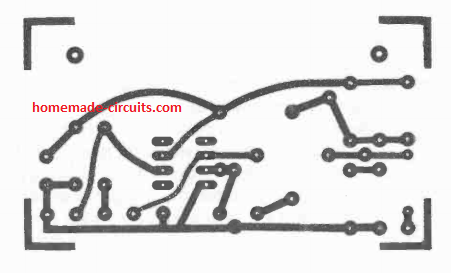
An additional type of resist are the rub-down etch resistant transfers which are available from several component merchants and which often can provide truly outstanding and specialized outcomes as demonstrated in the following example.
Actually you may find that there are lots of chemicals that can be applied as the etchant, but the majority of these are hazardous for some reason or another and are not likely suited to home designed boards.
The Etchant
The etchant is a chemical which reacts with the exposed copper area of the copper laminate and breaks it down from the board. It is used for taking off the copper regions on the board which are not painted by the etch resist and the areas which do not contribute to the track layouts and pads.
The etchant typically employed for home developed boards is ferric chloride, and while this is less hazardous compared to the majority of the choices, it is nevertheless a chemical that needs to be implemented with caution.
This should hence always be rinsed off quickly with running tap water in case you spill any on your skin. Make sure you don’t store ferric chloride in metallic containers, since this chemical is reactive to metals and make the metal porous and cause leakages.
As ferric chloride is toxic (and in in the course of many uses progressively gets transformed into copper chloride which is likewise extremely poisonous) it must obviously be stored far from foodstuff and utensils etc.
Types of Ferric Chloride
Ferric chloride can be obtained in a range of different forms. Probably the most handy type to have is a ready to use solution of the chemical. Many component suppliers market it in such liquid form; typically in 250ml containers and in a concentrated form.
You must dilute it a bit prior to use, as per the given guideline on the bottle. It may not require a great deal of dilution, and a 250ml bottle normally allows only 500ml or a litre after diluting it with water.
Some companies may provide the ferric chloride as crystals, also known as “Ferric Chloride Rock” sometimes. This label is very suitable since in this form it certainly looks like pieces of yellow rock rather then tiny nice crystals, which is pretty much rock solid.
In this type ferric chloride is normally available in 500gm packages, which is enough to generate one litre of etching solution.
You can as well get this in bigger packages, but since 500gm is enough to etch a seriously great number of regular size boards and may easily survive even an diligent constructor a very long time it is most likely not rewarding getting bigger than 500gm pack altogether.
How to Create Ferric Chloride Solution
In crystaline condition ferric chloride is not going to dissolve easily in particular, however when it is stirred steadily it may sooner or later break down completely, and with constant mixing it may melt fairly quickly.
Last but not least, ferric chloride can be acquired in anhydrous form, which basically signifies it’s genuine ferric chloride with virtually no water material. It will possess a slight degree of water in its crystalline form as an aside.
What actually causes this type of ferric chloride so hard to work with is the heating effect that is generated when it is mixed with water. Even if you begin with cooled water it can quickly become quite hot to a level at which the container turns very warm to touch, posing a danger of melting for plastic containers.
One more concern is that of having the chemical to dissolve adequately and create a decent etching formulation. For whatever reason you may find yourself ending up with a large quantity of chemical that will never break down, and also solution which appears like ferric chloride but has very little if any etching potential.
That is why cool water (ideally refrigerated or with ice) must be employed. It is additionally possible that there might be a tiny amount of chemical that won’t melt, which can either be strained from the liquid, or as it does not appear to impede etching it could simply be left in the solution.
Drill Bit Size
The next important ingredient for manufacturing PCB at home is the drill bit, which is required for drilling holes on the PCB for the component leads.
The typical diameter for component lead holes is 1mm, though a number of components like preset resistors, big electrolytic capacitors, etc. demand a bit bigger diameter. A hole diameter of about 1.4mm is appropriate for these kinds of components.
Typically, it is recommended to use a diameter of under 1mm for semiconductors and a number of other components that have thinner leads. 0.7mm or 0.8mm appear to be acceptable diameter for these components.
In case you have access to high quality drill bits they must be pretty tough.
However drill bits of around 0.7mm to 1.4mm in diameter may be quite weak and should be handled relatively carefully.
If they are maintained with downwards straight vertical pressure it may be fine, but if the orientation is not maintained at right angles to the board a proper hole won’t be created which is quite possible that the drill bit will break in two.
You have to for that reason take realistic care while drilling holes using such drill bits, and preferably the machine should be used with a adjustable stand as shown below.
We have so far discussed the key things which are necessary while making a printed circuit board, and there may be some other probabilities and ends which might be essential.
These are typically basic domestic objects though, and these will be unveiled as we advance with the etching course of action. You will find many different methods for manufacturing a printed circuit board.
Despite the fact that all of them are fundamentally the identical and the major dissimilarities are just the sequence through which the different measures along the way are performed.
We are going to hence begin by taking into consideration one approach of manufacturing a board, after which a couple of alternate techniques will be explained.
Getting Started with PCB Making
The very first step would be to check with the book or magazine where the printed circuit is presented in order to get the right dimensions of the board.
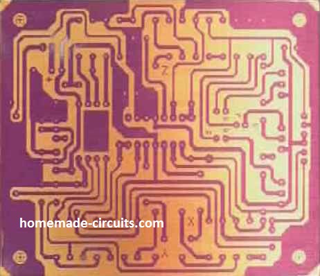
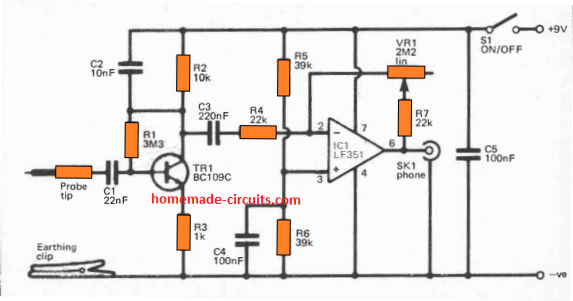
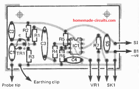
You might generally have a circuit schematic, a component overlay diagram, and the printed circuit track pattern reproduced in actual size, as given in the following 3 figures respectively.
The size of the printed circuit should be available in the text or the schematic, however in many instances it will be required to consider the proportions through the real size copper track pattern.
Mark the boundary of the finalized board on the copper side of the laminate board, then pull an additional set of lines approximately 2mm or so on the outer side of the previous marking.
By cautiously cutting between these outlines you should be able to generate a section of board with decent precision and straight edges with minimum issues.
The sides of the board could be smoothed using a small flat file, and with fibre glass board that eliminates the abrasive ends which can be undesirable.
Be aware that the markings should be done on the copper side of the board and sawn from the same side to prevent peeling of the copper while cutting the board. Therefore, make sure to cut, or drill the board always from the copper side, and not from the laminate side
The next step would be to draw the positions of the holes for the components, and wherever suitable, the fitting holes for the board mounting.
The quick method to get this done is to clamp the schematic drawing over the board on the copper track, by accurately aligning the drawing and the board edges.
Then, with a bradawl or similar pointed tool carefully and accurately marking through the schematic onto the board by punching small indentations in the copper.
It is not necessarily essential to mark the board by punching with a pointed tool, and an alternate way is to simply align and stick the drawing to the board using cello tape, and then drill down through the drawing which now itself acts like drilling markers.
Painting the Tracks with Etch Resist
After the board is trimmed to size and all holes drilled, the next task is to paint the board with the etch resist. This basically involves cleansing the board as extensively as you can.
Special cleaning blocks can be obtained from the market and these apparently perform quite nicely. Copper laminate boards may generally show some oxide and corrosion on top of the copper surface, and it is very important to remove this or else this may prevent the board from getting properly etched.
Hence, it is recommended to make use of a reasonably powerful cleaning agent which will perfectly eliminate all oxide, dirt and corrosion from the copper surface.
After the board has been comprehensively washed and the copper layer appears glistening throughout, rinse the board beneath warm water to get rid of any remnants of the cleanser or oily ingredient. At this point make sure not to touch the copper surface, which might otherwise cause greasy finger marks and slow down the etching process.
Next, take the etch resist paint to pull copper pads round the holes drilled for the components leads.
After the pads are drawn with etch resist, it’s time to paint the copper tracks so that they link up the pads as per the circuit design. Always make sure to keep your hands away from the copper surface while doing this. Begin from the board one edge and proceed systematically towards the other edge, instead of doing it randomly (which might likely result in mistakes)
For Complex PCB Designs
Several contemporary printed circuit designs can be extremely sophisticated and challenging to replicate.
While designing a board of this kind it is recommended work with a printed circuit resist pen (or a appropriate alternative) with an even finer nib. In places that may have many narrow, tightly packed parallel tracks, you must take the help of a ruler to allow fine straight lines to be sketched.
If you see the tracks or pads merging with each other, wait for the resist to dry up and then make use of a compass point or other sharp pointed to scratch away the excess overlapping resist.
As soon as the resist has dried out and the PCB is inspected, the next task is to submerge the board in the etchant solution until eventually all the exposed copper has been taken off.
How PCB Etching Happens
Essentially what goes on in the course of etching is that the copper takes the place of the iron in the ferric chloride to form copper chloride, while the iron gets precipitated.
In the beginning etching process happens pretty fast and could take only a few minutes, but as the ferric chloride progressively gets transformed into copper chloride the etching action steadily becomes sluggish, and after several boards are etched it can be observed that the etching time is rather prolonged, or not getting accomplished at all.
In that case the etchant will need to replaced with new batch of ferric chloride solution. As you will notice that Ferric chloride has a red-yellow color while copper chloride is blue in color, so when you find the etching solution slowly getting towards more greenish, will indicate that the chemical is nearing the finish of its working life.
While etching the board at home in a small dish make sure the copper side of the board is facing up and the process is carried out in a non-metallic dish having adequate size.
You may want to add a decent cover on top and periodically remove the cover to check the outcome until etching is over. A main problem with this method is that an iron and copper chloride layer tends to develop on top of the board which may significantly prolong the etching time. This may be countered by carefully rocking the dish from time to time to displace off this layer so that the etching speeds up.
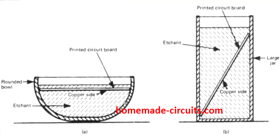
Using Special Containers for Etching
You may actually find it rather easy to set up a container in order to enable the PCB close to a vertical position with the copper side of the board facing downwards.
In this situation etching process happens really fast since iron precipitate is unable to develop a layer and tends to fall downwards away from the board. This ensures that the etching is not hampered. Still , periodic agitation of the board and etchant can help to knock off any small suppressing coating that may develop, enabling even faster etching.
Figure above shows a few easy options for accomplishing this. In Figure (a) a curved dish is employed which ensures that the board is maintained in place through the four corners, and does not come in contact with the dish at any other points.
The technique demonstrated in (b) a good choice for bigger PCBs which may necessitate a rather huge dish to enable the procedure. The container has to be pretty sizeable, anything similar to a classic instant coffee jar would work.
A great deal of etchant will probably be required so as to practically fill up the jar. This might look a bit pricey at first, however the etchant will certainly last proportionately more time compared to a smaller quantity.
Alternatively, a lesser amount of etchant can be diluted with higher amount of water, but this could considerably decelerate etching and is not advisable.
For substantially large boards the only functional method of etching the board could be to employ a big flat dish (like a photographic dish) with the copper side facing upwards. Frequent agitation may be accustomed to speed up the etching time.
Etching will be seen happening faster on areas of where there are smaller regions of open copper, and will take a lot longer on areas of the board where there are relatively wider areas of open copper. Etching also takes place more quickly round the perimeters of the board.
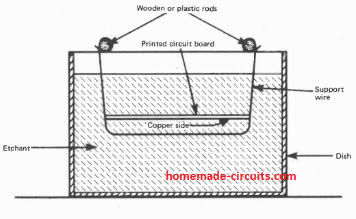
A method which usually works more effectively and is typically far easier in practice is displayed above. Here a pair of wooden or plastic rods are put down the entire length of the dish, on opposite sides. These are relatively longer than the dish to allow them to rest on top. The board is then hung from the rods supported on a couple of wire pieces, one at each end of the board.
Just a single wire is demonstrated in Figure for better understanding. If copper wire is used make sure it is a super Enameled copper wire having a thickness of 18 SWG. The wires are attached to the rods simply by turning the ends round the diameter of the rod once or twice.
After Etching is Over
When etching appears to be complete, you must thoroughly examine the board to make sure that there are no pockets of open copper left, and look for parts of the board where the copper tracks and pads are closely drawn (for example groupings of IC pads).
After you have confirmed that etching is totally accomplished, keep the board vertically over the etching solution for some moments to allow the dripping etchant elope the board, and then wipe the board using a piece of tissue paper or rag.
As an aside, this is a wise decision to maintain a piece of kitchen paper nearby throughout the etching process to ensure that remnants of etching solution could be wiped from the tweezers or gloves whenever needed. The board must be then carefully washed in water to launder away any final leftover traces of etching solution.
Removing the Resist
Finally at the end, the resist sticking on the copper has to be eliminated, that might otherwise seriously impede the soldering process on the copper pads. You can acquire any standard resist remover, and this may be in the form of a light spirit that will break down the majority of paints and inks.
It may be also feasible to obtain printed circuit polishing blocks that happen to be likewise well suited for scrubbing of the resist. One more technique is to try using a scouring pad or powder, and this is basically among the most straightforward activities of printed circuit production which should certainly not present any kind of challenges.
To enable the final assembly of the components on the ready PCB with perfect soldering and absolutely no “dry” joints, the copper tracks and pads must be polished to a glossy finishing before the soldering of the components can be actually commenced.
Over to You
As explained above, apparently making PCB at home looks pretty simple, and it is just a matter of a few hours to create outstanding professional grade PCBs using ready made DIY materials from the market. That said, the process may require some caution and precision for achieving the desired results, so that the intended circuit project is accomplished successfully.
If you have any doubts regarding the topic, please let us now through the comments below, we’ll be most happy to help!
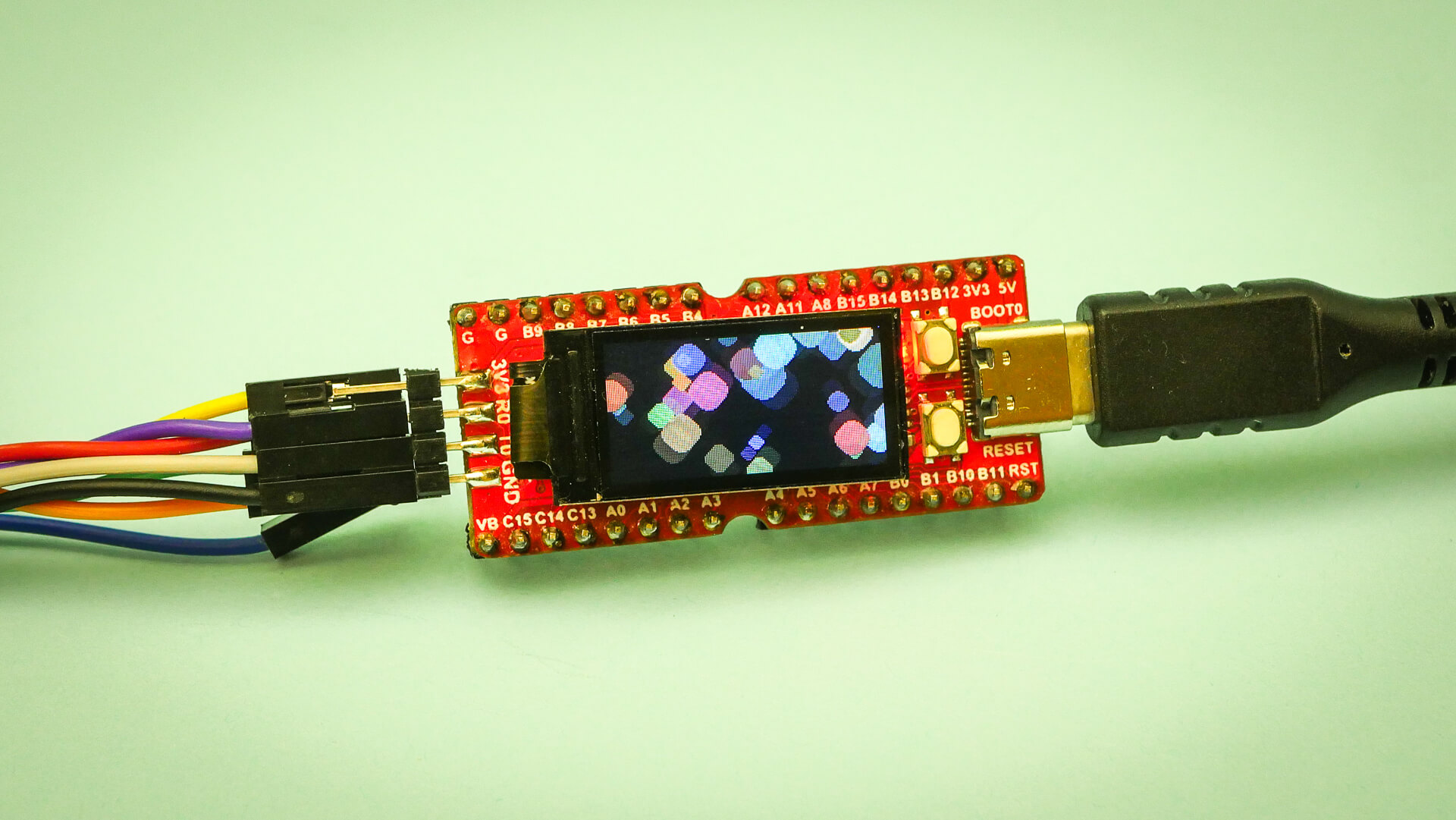
RISC-V is gaining traction and some development boards have already popped up. One of them is the widely available Sipeed Longan Nano. Written information is a bit sparse at the moment. Let’s try to fix this with a quick writeup on wiring and programming the board. If you just want to see what the board can do here is a video instead.
Nuclei SDK
For programming a GD32V series SoC best choice at the moment is the Nuclei SDK. It seems to be well maintained, exceptionally well structured and is quite easy to learn. Developing is done with your favourite text editor.
The SDK supports three different real time operating systems: FreeRTOS, UCOSII and RT-Thread. Since Longan Nano has only 32kB SRAM you might want to stay baremetal instead.
Nuclei SDK does support Longan Nano out of the box. Basic hello world and the Makefile would look like this.
You would compile and upload it with the following commands.
$ make SOC=gd32vf103 BOARD=gd32vf103c_longan_nano all
$ make SOC=gd32vf103 BOARD=gd32vf103c_longan_nano upload
The SDK will take care of basic things such use redirecting STDOUT to USART. This is where the Sipeed USB-JTAG/TTL RISC-V Debugger really pays off. In addition to the JTAG interface it also acts as an USB to TTL converter.
$ screen /dev/ttyUSB1 115200

Nuclei SDK Build Time: Nov 14 2020, 23:17:41
Download Mode: FLASHXIP
CPU Frequency 108540000 Hz
Hello world
Uploading with the Sipeed RISC-V debugger
To make both JTAG and serial interface work you need to connect all pins except NC (duh!) between the debugger and Longan Nano. If nitpicking second ground is also optional. Longan Nano RST is pin number 7 on the left side of the USB socket.
Debugger
Longan Nano
GND
GND
RXD
T0
TXD
R0
NC
GND
GND (optional)
TDI
JTDI
RST
RST
TMS
JTMS
TDO
JTDO
TCK
JTCK
When flashing you also need to connect the USB-C socket to provide power. When using Nuclei SDK you can flash the firmware with make.
$ make SOC=gd32vf103 BOARD=gd32vf103c_longan_nano upload
Uploading with the J-Link debugger
Debugger
Longan Nano
VREF
3v3
GND
GND
TDI
JTDI
RST
RST
TMS
JTMS
TDO
JTDO
TCK
JTCK
You can also use SEGGER J-Link Commander to upload the firmware. The command line utility requires the firmare to be in hex format.
To upload a new firmware manually, first halt the CPU and load the firmware.hex from above. Reset the core and peripherals. Set the program counter to 0x08000000 and finally enable the CPU and exit the command line utility.
If the new firmware does no run automatically you might need to powercycle the board.
While manually poking the internals might be fun it gets bothersome in the long run. You can also put the above commands to an external file and pass it to JLinkExe to do all of the above automatically.
$ cat upload.jlink
halt
loadfile firmware.hex
r
setPC 0x08000000
go
q
If you don’t have an external debugger it is also possible to upload via USB. At the time of writing you need to use latest dfu-util built from source.
$ git clone git://git.code.sf.net/p/dfu-util/dfu-util
$ cd dfu-util
$ ./autogen.sh
$ ./configure --prefix=/opt/dfu-util
$ make -j8 install
Then add /opt/dfu-util/bin to your $PATH and you should be able to flash the firmware via USB.
$ make SOC=gd32vf103 BOARD=gd32vf103c_longan_nano bin
$ dfu-util -d 28e9:0189 -a 0 --dfuse-address 0x08000000:leave -D firmware.bin
Before running dfu-util you need to put the board to download mode. Do this by holding down the BOOT and RESET buttons and then release the BOOT button to enter download mode.
Hello World on Screen
For graphics programming you could use HAGL. As the name implies HAGL is a hardware agnostic graphics library. To make it work with Longan Nano you also need a HAGL GD32V HAL
Writing directly to display is fine for unanimated content. However above code will have a horrible flicker. Problem can be fixed by enabling double buffering in hte Makefile.
COMMON_FLAGS += -DHAGL_HAL_USE_DOUBLE_BUFFER
With double buffering enabled we also need to flush the contents from back buffer to display ie. front buffer. Here I also add some delay to slow down the animation.
This is very naive approach and you need to manually adjust the delay to avoid tearing. It would be better to implement an fps limiter and flush the contents, for example 30 times per second.
A much higher level of randomness can be obtained by observing some aspect of the real physical world, and capturing a noisy signal (“noise” == “random” in physics … sort of).
With an ADC, this is easy to do: leave one ADC input pin floating, and measure its analog voltage. The least-significant bit will be the noisiest, always fluctuating due to electrical noise, e.g. the omni-present thermal brownian motion. If we repeat this 32 times and keep only the lower bit, we should get nicely random results:
ADC<0> adc;
PinA<0> floatingPin;

uint32_t randomNumber () {
    uint32_t r = 0;
    for (int i = 0; i < 32; ++i)
        r = (r << 1) | (adc.read(floatingPin) & 1);
    return r;
}